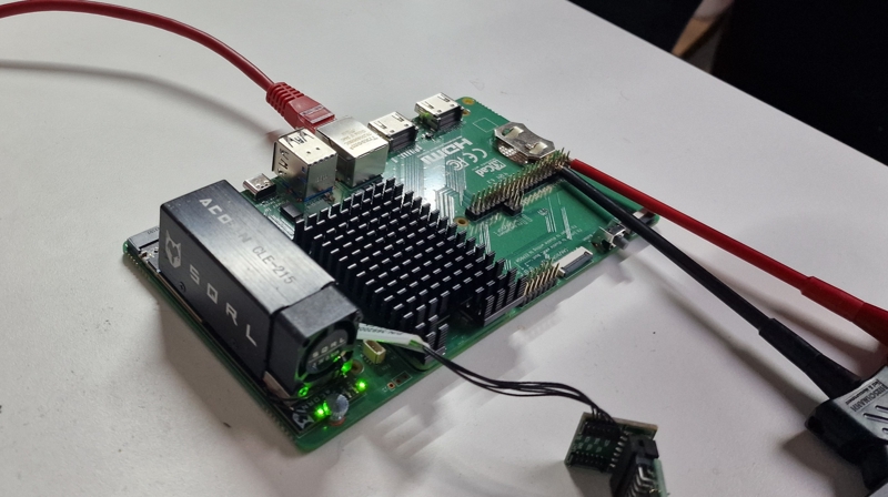
A while ago I bought myself a NiteFury-II FPGA board to be able to perform development with PCIe interfacing. The Nitefury/Litefury project is a spin-off from RHSResearchLLC, developed by former members of Acorn CLE. Alongside the FPGA board I bought a Raspberry Pi Compute Module (CM) 5 including an IO board which is equipped with a M.2 M-key connector. The Nitefury-II uses a Xilinx Artix A7-200T which is put into a M.2 M-key form factor PCB which fits perfectly on the IO board. The FPGA also has access to 1GiB of DDR3-800MHz (1600MT/s) which can be used with Xilinx’s Memory Interface Generator (MIG) IP. The board is equipped with 4 user controlled LED’s (A1-A4). Unfortunately the Raspberry PI CM5 has only one PCIe Gen 2 lane routed to the IO board’s M.2 connector. This gives us a maximum theoretical bandwidth of 5GT/s (625MB/s) while the board is equipped with 4 lanes of PCIe gen 2. For my testing purposes the lower bandwidth doesn’t really bother me as 5GT/s is still a sufficient amount of bandwidth.
So let’s equip the IO board with the FPGA accelerator and create our first FPGA image.
FPGA Design#
To be able to experiment and demonstrate something, I need to have a working FPGA image. For the creation of a FPGA image, I used Vivado’s Block Diagram for easy integration. For the PCIe core I used the XDMA IP from Xilinx which is free to use. The XDMA core was configured to interface via AXI4-Lite and AXI4-Stream. For the AXI-Lite interface, I chose to use a BRAM and a GPIO peripheral for easy and more visual testing. The BRAM peripheral is configured only as a RAM pool, it has no meaningful purpose. The GPIO peripheral is connected to 3 of the 4 user LEDs on board. For the AXI4-Stream interface, one host-to-card (H2C) port and one card-to-host (C2H) port was setup in loopback with a AXI4-Stream FIFO in between to experiment with AXI4-Stream and PCIe.
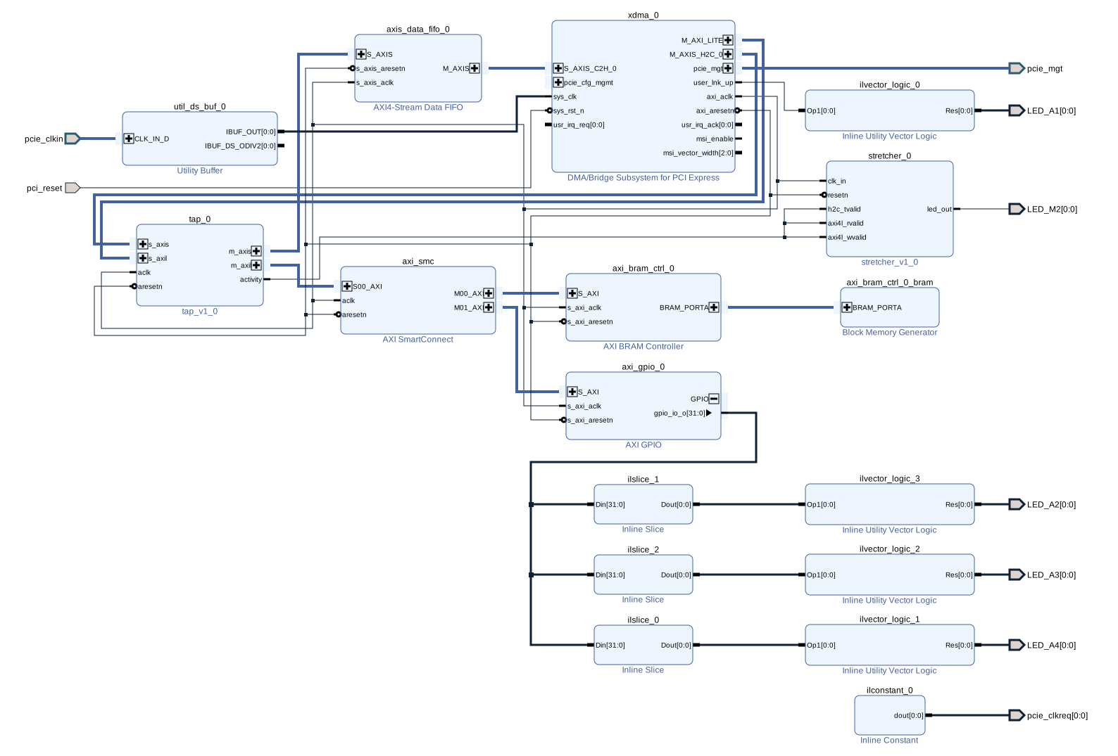
The clocking network is driven by the PCIe differential reference clock from the compute module.
After a long time of troubleshooting of why the FPGA board didn’t get a clock signal, I discovered the existence of the PCIe clkreq signal.
The PCIe clkreq signal is an active low signal that sends a request to the PCIe root complex to gate the clock to our peripheral.
The clock gating functionality is to save power when the peripheral enters a sleeping state and to distribute a clock signal only when necessary.
The clkreq signal is availabe to a GPIO on our FPGA board such that we can pull the clkreq signal low to request a clock reference.
The M.2 M-key connector also has a special pin called Device Activity Signal (DAS) which in the case of the IO board is connected to an activity LED. The DAS signal is available to a FPGA GPIO such that we can toggle the LED to signal bus activity. My plan was to connect the LED to the TVALID signal of the H2C streaming interface and a couple of xVALID signals of the AXI4-Lite interface. Unfortunately these valid signals switch so fast that it is hard to notice the activity. The LED is always on or off which does not give a clear indication of bus activity. To solve this issue I wrote a simple pulse “stretcher” module that ensures the LED can blink at 10Hz on activity. Another problem was that when connecting the valid signals to the stretcher module, Vivado informed that the block diagram interface signals will not get connected which was an actual problem. For this I ended up writing a simple VHDL tap module which was able to tap these signals of the interface signals.
As an end result, I ended up with 3 user controlled LEDs (LED A2 to A4) via the GPIO peripheral, one M.2 DAS LED, a BRAM peripheral, an AXI4-Stream loopback and a link status LED (LED A1).
Pulse Strecther Module:
After succesfully running the synthesis and implementation I created a MCS file and succesfully flashed the image onto the FPGA flash chip.
First boot#
Let’s power up the system and see if the compute module is able to find our PCIe device. The link status LED (A1) is turned on which is a good sign.
$ lspci
0001:00:00.0 PCI bridge: Broadcom Inc. and subsidiaries BCM2712 PCIe Bridge (rev 30)
0001:01:00.0 Processing accelerators: Xilinx Corporation 7-Series FPGA Hard PCIe block (AXI/debug)
0002:00:00.0 PCI bridge: Broadcom Inc. and subsidiaries BCM2712 PCIe Bridge (rev 30)
0002:01:00.0 Ethernet controller: Raspberry Pi Ltd RP1 PCIe 2.0 South Bridge
And there it is, our custom PCIe device! Before we can do anything useful we need to download, install and load the XDMA Linux kernel module from Xilnx.
Driver installation:
$ git clone https://github.com/Xilinx/dma_ip_drivers.git
$ cd dma_ip_drivers/XDMA/linux-kernel/xdma
$ make
$ sudo make install
Load driver and see if it is loaded:
$ modprobe xdma
$ lsmod | grep xdma
xdma                  131072  0
There it is, the kernel module is succesfully loaded!
Experimenting#
Now that we got ourself a functional driver, Let’s see what we can do with the functionality on board of the FPGA.
AXi4-Lite GPIO peripheral#
To let the GPIO’s do something meaningful, I wrote a simple C-program which MMAP’s to the /dev/xdma_user character device to be able to memory map to the configured BAR.
Now that we are able to do direct memory mapped transactions, we can toggle the 3 (A2-A4) configured LEDs.
The C program performs a simple addition to the GPIO register every 100ms which shows a 3-bit binary counter on the LEDs.
Let’s compile the program and run it to see the GPIO binary counter in action!
$ gcc main.c -o main
$ ./main
Running 3-bit counter!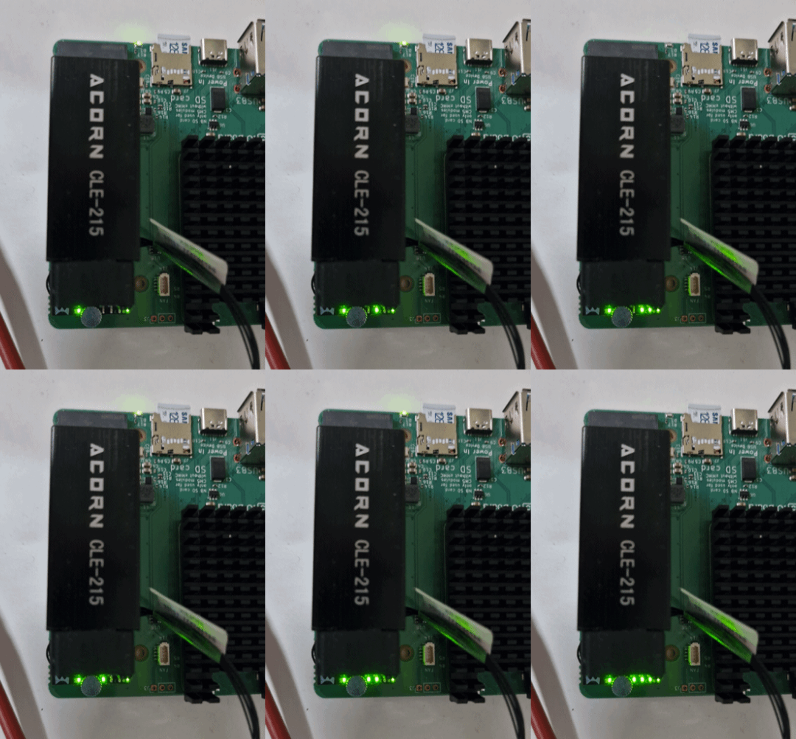
As can be seen in the GIF above, the binary counter works and the M.2 DAS activity LED on the right top blinks as well.
AXI4 BRAM Controller#
For the BRAM controller I implemented a C program that is able to write a text string into memory and able to read the result back out.
The following program arguments are available for the user:
- Write option: The user provides a text string which will be written into the BRAM.
- Read option: The text string in memory gets printed into the terminal.
For this program I had to perform some string case conversion and basic parsing to be able to determine which option to execute.
Let’s try our program:
$ sudo ./bram write "I am Randy"
Executing BRAM test
Wrote: "I am Randy", into BRAM!

$ sudo ./bram read
Executing BRAM test
I am RandyAXI4-Stream#
Let’s start exploring the AXI streaming interface.
I thought it would be fun to stream some real data through the interface so I wrote a simple hello world C program called hello.c which will be sent through the loopback, back into a C file.
#include <stdio.h>

int main(int argc, char const *argv[]) {
    printf("Hello World via AXI4-Stream!\n");
    return 0;
}
At the transmitting side (H2C) we pipe the hello.c file into the device and at the receiving end (C2H) we pipe the output into a test.c file.
$ dd if=hello.c of=/dev/xdma0_h2c_0
$ dd if=/dev/xdma0_c2h_0 of=test.c
Now Let’s cat the file:
$ cat test.c
#include <stdio.h>

int main(int argc, char const *argv[]) {
    printf("Hello World via AXI4-Stream!\n");
    return 0;
And voila there is our test.c file, streamed through the AXI4-Stream loopback interface!
Let’s try to compile the program and see if there are no corupt artifacts like invisible characters.
Compile and run:
$ gcc test.c -o test
$ ./test
Hello World via AXI4-Stream!Conclusion#
This project successfully demonstrated PCIe communication between a Raspberry Pi CM5 and a Xilinx FPGA through the XDMA interface. I had a lot of fun during this experiment and I learned a lot.
Some key takeaways from this experience:
- PCIe clock request (clkreq) signal management is essential for proper operation
- The XDMA Linux kernel driver provides straightforward access to custom AXI enabled FPGA peripherals
- The AXI4-Stream interface enables high-throughput data transfers with minimal CPU overhead via the DMA
The setup successfully achieved data transfers through the loopback interface, validating the design approach. While limited to a single PCIe Gen 2 lane, the 5GT/s bandwidth proved more than sufficient for testing purposes.
Next steps for this platform include designing and implementing a kind of crypto miner perihperal.